 |
|
|
 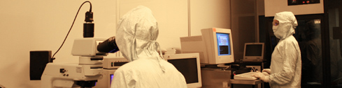 |
Process Specialties was founded in 1988 by experienced process engineers on one principle, to provide our clients with the most consistent, and the highest quality semiconductor processing services available. For 35 years we have specialized in device quality thin film deposition, Photolithography and confidential research & development processing. We have built our reputation on our dedication to quality, confidentiality and customer service. Over the years the word has spread to companies across the world. Now over 50 leading edge companies around the world use our thin films and processes for everything from advanced semiconductor tool and process development, to OEM standards, MEMS, medical-genome devices and foundry device manufacturing. Our thin films and processes are so reliable and consistent, major U.S. metrology tool manufacturers use us to build their internal and external OEM thin film standards. We have often been called "the Industry Standard" in thin film processing. When you call PSI you will speak to one of our helpful technical service representatives, or a competent device engineer that can answer your tough processing questions. You will find we offer a wide range of in-house processing services. In our Fab areas we maintain strict statistical process control and complete documentation. This allows you to receive the same reliable processing month after month, and year after year on your thin film or custom process. | |
 |
Process Specialties is proud to celebrate its 35th year in business! |
| CONTACT PSI | © 1996-2023 Process Specialties Inc., all rights reserved |